(China (Mainland))

Product Summary
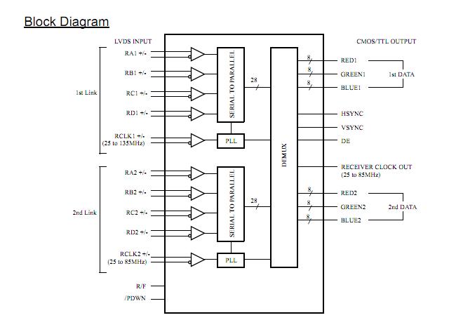
The THC63LVD824 is a receiver designed to support Single Link transmission between Host and Flat Panel Display up to SXGA+ resolutions and Dual Link trans- mission between Host and Flat Panel Display up to UXGA resolutions. The THC63LVD824 converts the LVDS data streams back into 48bits of CMOS/TTL data with falling edge or rising edge clock for convenient with a variety of LCD panel controllers.
Parametrics
THC63LVD824 absolute maximum ratings: (1)Supply Voltage (VCC): -0.3V ~ +4.0V; (2)CMOS/TTL Input Voltage: -0.3V ~ (VCC + 0.3V); (3)CMOS/TTL Output Voltage: -0.3V ~ (VCC + 0.3V); (4)LVDS Receiver Input Voltage: -0.3V ~ (VCC + 0.3V); (5)Output Current: -30mA ~ 30mA; (6)Junction Temperature: +125℃; (7)Storage Temperature Range: -55 ~ +125℃; (8)Lead Temperature (Soldering, 10sec): +230℃; (9)Maximum Power Dissipation @+25℃: 1.0W.
Features
THC63LVD824 features: (1)Wide dot clock range: 25-170MHz suited for VGA, SVGA, XGA, SXGA, SXGA+ and UXGA; (2)PLL requires No external components; (3)Supports Single Link up to 135MHz dot clock for SXGA+; (4)Supports Dual Link up to 170MHz dot clock for UXGA; (5)50% output clock duty cycle; (6)TTL clock edge programmable; (7)TTL output driverbility selectable for lower EMI; (8)Power down mode; (9)Low power single 3.3V CMOS design; (10)100pin TQFP; (11)THC63LVDF84B compatible.
Diagrams
| Image | Part No | Mfg | Description |  |
Pricing (USD) |
Quantity | ||||
|---|---|---|---|---|---|---|---|---|---|---|
 |
 THC63LVD824 |
Other |
|
Data Sheet |
Negotiable |
|
||||
| Image | Part No | Mfg | Description | |
Pricing (USD) |
Quantity | ||||
|
THC63LVD103 |
Other |
|
Data Sheet |
Negotiable |
|
||||
|
THC63LVD104A |
Other |
|
Data Sheet |
Negotiable |
|
||||
|
THC63LVD104S |
Other |
|
Data Sheet |
Negotiable |
|
||||
|
THC63LVD823 |
Other |
|
Data Sheet |
Negotiable |
|
||||
|
THC63LVD824 |
Other |
|
Data Sheet |
Negotiable |
|
||||
|
THC63LVDF64A |
Other |
|
Data Sheet |
Negotiable |
|
||||