Product Summary
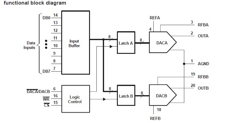
The TLC7528CDWR is a dual, 8-bit, digital-to-analog converter (DAC) designed with separate on-chip data latches and feature exceptionally close DAC-to-DAC matching. Data of TLC7528CDWR are transferred to either of the two DAC data latches through a common, 8-bit, input port. Control input DACA/DACB determines which DAC is to be loaded. The load cycle of TLC7528CDWR is similar to the write cycle of a random-access memory, allowing easy interface to most popular microprocessor buses and output ports.
Parametrics
TLC7528CDWR absolute maximum ratings: (1)Supply voltage range, VDD (to AGND or DGND): -0.3V to 16.5V; (2)Voltage between AGND and DGND: ±VDD; (3)Input voltage range, VI (to DGND): -0.3V to VDD + 0.3; (4)Reference voltage, VrefA or VrefB (to AGND): ±25V; (5)Feedback voltage VRFBA or VRFBB (to AGND): ±25V; (6)Input voltage (voltage mode out A, out B to AGND): -0.3V to VDD+0.3; (7)Output voltage, VOA or VOB (to AGND): ±25V; (8)Peak input current: 10μA; (9)Operating free-air temperature range, TA: 0℃ to +70℃; (10)Storage temperature range, Tstg: -65℃ to +150℃; (11)Case temperature for 10 seconds, TC: FN package, +260℃; (12)Lead temperature 1,6mm (1/16 inch) from case for 10 seconds: DW or N package, +260℃.
Features
TLC7528CDWR features: (1)Easily Interfaced to Microprocessors; (2)On-Chip Data Latches; (3)Monotonic Over the Entire A/D Conversion Range; (4)Interchangeable With Analog Devices AD7528 and PMI PM-7528; (5)Fast Control Signaling for Digital Signal Processor (DSP) Applications Including Interface With TMS320; (6)Voltage-Mode Operation; (7)CMOS Technology.
Diagrams

| Image | Part No | Mfg | Description |  |
Pricing (USD) |
Quantity | ||||||||||||
|---|---|---|---|---|---|---|---|---|---|---|---|---|---|---|---|---|---|---|
 |
 TLC7528CDWR |
 Texas Instruments |
 DAC (D/A Converters) 8bit .1us 5-15V |
 Data Sheet |

|
|
||||||||||||
 |
 TLC7528CDWRG4 |
 Texas Instruments |
 DAC (D/A Converters) 8-Bit 0.1 us Dual MDAC |
 Data Sheet |

|
|
||||||||||||
 (China (Mainland))


